


Optical Thin Films Encyclopedia: Interference, Design Software and Coating Processes Explained
Optical thin films are the soul of components such as lasers, field lenses, protective windows, cavity mirrors and beam splitters. Coat the same piece of glass correctly and it is a transmissive element; coat it wrong and it becomes a source of loss or even damage in the optical path. Yet many plausible-sounding claims circulate in the industry — about vacuum level, pump selection and what software can do — and many practitioners remain unsure to this day.
This article explains optical thin films in the order ‘principle → software → process → selection → misconceptions’. All data come from RP Photonics, Excelitas white papers, TFCalc official material, GB/T 3224 national standard and public reports of the 1064 nm thin-film damage competition, with sources noted throughout. Parameters are typical engineering values; actual selection must follow specific conditions and measured data.
If you remember only three things: ① every function of a thin film comes from interference, with quarter-wave thickness solving the phase condition and index matching solving the amplitude condition; ② coating ‘vacuum level’ must distinguish base pressure from working pressure — they are not the same; ③ in high-power laser scenarios the laser-induced damage threshold (LIDT) matters more than reflectance.
Contents
- 1. What Are Optical Thin Films: Core Concepts and a Three-Layer Framework
- 2. Working Principle: How Interference Delivers AR, HR and Beam Splitting
- 3. Design Software: TFCalc, Essential Macleod and OptiLayer Compared
- 4. Coating Processes: Choosing Between Evaporation, Magnetron Sputtering and Ion Plating
- 5. Vacuum Systems: Base Pressure and Working Pressure Must Be Distinguished
- 6. Laser-Induced Damage Threshold: 1064 nm High-Power Coating Parameters and Practice
- 7. Quick Selection Guide: Working Back from Application to Film and Process
- 8. Common Misconceptions: Six Widespread False Claims
1. What Are Optical Thin Films: Core Concepts and a Three-Layer Framework
One-sentence definition: an optical thin film is one or more nanometre-scale layers deposited on a substrate such as glass, crystal or metal by physical or chemical means, to control reflection, transmission, polarisation, phase and spectral distribution as required.
The film is only tens to hundreds of nanometres thick — an A4 sheet is about 100 μm, i.e. 1000 nm, enough to hold a hundred such films. Yet something this thin determines a laser’s output efficiency. What is hard to grasp at first is that it is phase, not thickness itself, that does the work.
To understand a film design you must look at three levels at once; missing one leads to a wrong judgement:
| Level | Question addressed | Key variables | Consequence of getting it wrong |
|---|---|---|---|
| Physical level How interference happens |
How light interferes between film layers | Refractive index n, extinction coefficient k, optical thickness nd, layer count, incidence angle | Calculated spectrum completely fails to match measurement |
| Process level How it is deposited |
Whether the design can be reproduced by the process | Deposition temperature, rate, ion energy, substrate roughness, chamber cleanliness | Porous, moisture-absorbing, stressed films with poor batch consistency |
| Reliability level Whether it survives the operating environment |
Whether the film is stable under working conditions | LIDT, environmental stability, adhesion, abrasion resistance | The film cracks or is damaged in service |
The industry saying ‘however good the design, it is useless if you cannot make it’ describes exactly the constraint between these three levels. Design software computes an ideal spectrum; the real film is a product of the process, and the gap is the superposition of process tolerance and measured film-material deviation.
For the specific film types (AR anti-reflection, HR high-reflection, BS beam splitting, AT attenuating-splitting, FI bandpass, PBS polarising splitting, PC polarisation holding, etc.), there is a dedicated article on codes and applications on this site: Common Functions of Optical Thin Films: HR, AR, BS, AT, FI, PBS, PC. This article focuses on principle, process and selection and does not repeat the type list.
2. Working Principle: How Interference Delivers AR, HR and Beam Splitting
2.1 Two basic conditions for interference
Light reflects once each at the upper and lower interfaces of a film, forming two reflected beams R1 (upper-surface reflection) and R2 (lower-surface reflection). Their combined intensity depends on the phase difference and amplitude ratio between the two beams. The phase difference has two parts:
Δ = (phase-jump difference) + (2π × 2 nf d cosθt / λ)
The first term is one many people miss. It comes from the ‘half-wave loss’: when light reflects from an optically rarer to a denser medium, a π phase jump occurs. So the jump at each interface must be determined first — never assumed.
For a single-layer AR film, n0 < nf < ns, so both interfaces are ‘rarer to denser’, and each undergoes a π phase jump; the two jumps cancel, leaving the simplest case where only the propagation optical path difference must be arranged.
2.2 Full derivation of a single-layer AR film
Phase condition — the two reflected beams are in antiphase:
2 nf d = λ/2 → nf d = λ/4
This nf d = λ/4 is the quarter-wave optical thickness (QWOT), the starting point of AR film design. The propagation path difference between R1 and R2 is exactly half a wavelength; with the π jump common to both beams, the total phase difference is exactly π and they cancel.
Amplitude condition — the two beams have comparable intensity:
nf = √(n0 · ns)
Both conditions must be met simultaneously. Satisfying only the phase condition gives ‘less reflection’, not ‘reflection eliminated’ — a point many introductory articles gloss over.
What is achievable in practice? Take BK7 glass (ns = 1.52) with air (n0 = 1.0): the ideal nf = √(1.0 × 1.52) ≈ 1.23. But no solid material with so low an index exists in nature. The most common engineering choice today is magnesium fluoride MgF2 (n = 1.38):
| Item | Value | Notes |
|---|---|---|
| Design wavelength | 550 nm | Near the green centre of the visible band |
| Substrate / film material | BK7 / MgF2 | MgF2 n ≈ 1.38, one of the lowest-index practical film materials |
| Physical film thickness | 99.6 nm | About 0.1 μm, less than a thousandth of a hair’s width |
| Normal-incidence reflectance | 4.3% → 1.3% | Bare glass about 4.3%, down to about 1.3% after coating |
| Oblique-incidence effect | Shifts to 513 nm at 30° | At oblique incidence cosθt shortens the effective path, moving the reflectance minimum to shorter wavelengths |
Source: RP Photonics, Edmund Optics anti-reflection technical documents
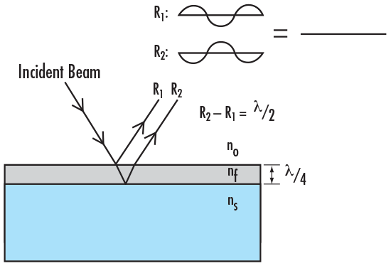
Image source: Edmund Optics ‘Anti-Reflection Coatings’ application guide
This is the practical ceiling of a single-layer AR film. To work over a broader band or at lower reflectance requires multilayer structures (V-coats, broadband AR / BBAR, etc.); only when layer counts rise do process difficulty and error accumulation become the real bottleneck.
2.3 Half-wave thickness and multilayer films
Besides QWOT, half-wave optical thickness (HWOT, nf d = λ/2) is another basic design unit. It introduces a π phase shift by itself and has three uses: compensating phase jumps, serving as the spacer layer in interference filters, and precisely tuning spectral phase in multilayers.
High-reflection films (HR) stack alternating high-index H and low-index L materials, each a quarter wave thick, forming an (HL)N structure. Designed well, reflectance can exceed 99.9%, the basis of laser cavity mirrors and interference filters. **An easily overlooked point: although each layer is λ/4, interference here is ‘all reflections added in phase’, the opposite logic to AR’s ‘cancellation’.** Confusing the two gives completely wrong layer-count estimates.
2.4 The beam-splitter approach
A beam splitter (BS) is essentially an interference filter: at the transmission peak (passband) the two transmitted beams add constructively, while in reflection the energy is divided in the designed ratio. Whether R:T is 50:50 or 90:10 depends on layer count, material combination and incidence-angle design. The hard part of interference-filter design is often not ‘whether it passes’ but how narrow the bandwidth can be made — for an ultranarrow filter with FWHM below 1 nm, even 1–2 nm of interface diffusion drops peak transmittance by 2%–5%.
3. Design Software: TFCalc, Essential Macleod and OptiLayer Compared
Thin-film design software does three things: compute spectra, optimise film designs and verify manufacturability. The third is most often overlooked, yet is the software’s real value over ‘hand calculation’.
| Software | Positioning and features | Core capabilities (including pitfalls) | Suitable scenarios |
|---|---|---|---|
| TFCalc Guangyan Tech / Hulinks |
Integrated tool for general film design and production analysis, with the lowest entry barrier | Up to 5000 layers on each side of the substrate (note: 5000 per side, not 5000 total on one face); supports layer-stack formulas such as (HL)51.2(HL)5; optimisation by variable-metric, gradient and simplex local methods, plus needle optimisation (with tunnel effect) and global search; tolerance sensitivity, yield analysis and cone-angle averaging; can simulate the output of a coater’s light monitor | Component shops taking daily orders, needing both design and proof to customers that ‘this film can be made’ |
| Essential Macleod | Integrated analysis-and-design software package with a multiple-document interface | Designs and optimises everything from single layers to precise splitter films; evaluates WDM/DWDM filters; supports design from scratch or optimisation of an existing design and estimates errors in the design; a product line over forty years old and one of the industry benchmarks in telecom filters | Design and verification of telecom filters and complex multilayers |
| OptiLayer | Covers the full ‘parameter–design–production–reverse-engineering’ flow, with the strongest modularity | Three clear modules: OptiLayer handles target merit functions, optimisation and pre-production error analysis; OptiChar reverse-engineers an optical-constants model matched to measurements and shows each factor’s influence; OptiRE reverse-engineers measured post-production spectra and feeds errors back to guide production; the three link through the OptiReOpt dynamic-link library (DLL), enabling a closed loop of design–modify–monitor in real time | Production lines needing a design–production–reverse-engineering loop and continuous tracking of process drift |
Source: TFCalc official feature list (Hulinks / Guangyan Tech)
3.1 Selection advice
For order-taking component shops TFCalc offers the best value, because it builds in yield analysis and light-monitor simulation — hard currency when quoting delivery. Telecom filters cannot do without Essential Macleod. Only lines truly needing a design–production–reverse-engineering loop and continuous tracking of film-material batch differences justify the cost of the OptiLayer suite.
3.2 Three easily overlooked software principles
① Always do tolerance analysis — never judge by the plotted curve alone. The target spectrum from design software assumes ideal parameters. In real production film thickness has errors and film-material n/k deviates from design values. Typical magnitudes: a V-type four-layer AR film with ±1% systematic thickness error at the centre wavelength drops peak transmittance from 99.8% to 99.3%–99.5%; for a 532 nm narrowband filter, 1% random thickness error can drop peak transmittance from 90% to below 85%, with broader FWHM and worse squareness. A design that plots beautifully but cannot withstand process error is a paper design, not a product.
② Tolerances in the merit function must match real process capability. Thickness-control precision varies greatly between processes — electron-beam evaporation, ion-beam sputtering and ion-assisted deposition (IAD) do not achieve the same thickness tolerance for the same design. Setting process tolerances too idealistically makes the optimiser return a plan the process cannot make.
③ Use measured n/k of the film material in software, not handbook values. The same material has systematic n/k differences under different deposition processes, especially as films thin down. Only optical constants measured under the actual process let design match measured spectra. This is the reason modules such as OptiChar exist.
4. Coating Processes: Choosing Between Evaporation, Magnetron Sputtering and Ion Plating
By film-forming mechanism, physical vapour deposition (PVD) falls into two broad classes: evaporation (material melted and vaporised) and sputtering (ions bombarding target atoms loose). Ion plating is not an independent third class — it is a plasma-enhancement means layered on evaporation. The three are at different levels and cannot be listed as ‘three heating methods’.
4.1 Evaporation
A resistance wire or high-frequency induction heats the crucible, vaporising the film material to deposit on the substrate; electron-beam evaporation (E-beam) heats the melt pool directly with an electron beam and can handle high-melting-point materials.
| Advantages | Simple equipment, low cost, high rate; suited to high-volume evaporation of metal films such as aluminium |
|---|---|
| Limitations | Conventional E-beam evaporation often deposits below 80 °C, giving porous films that absorb moisture; interface roughness is usually on the order of 1–2 nm |
| Suitable for | Metal mirrors, decorative coatings, non-critical optical surfaces; demanding cases require ion-assisted deposition (IAD) or ion-beam sputtering |
4.2 Sputtering
Ion-beam sputtering (IBS): an ion gun emits an ion beam that bombards the target at a set incidence angle, sputtering target atoms off to form a film. Film density and uniformity are good, and interface roughness can be kept below 0.5 nm — its value in high-precision coating. The price is a small bombarded area and low deposition rate, with throughput a hard constraint.
Magnetron sputtering: a magnetic field is applied to a DC or RF target face to constrain electron motion. The physical picture must be followed through:
Electrons emitted by the cathode target → accelerated by the electric field into the magnetic field above the target → confined into a high-density electron cloud circling the field lines → colliding with Ar atoms to ionise large numbers of Ar+ → Ar+ bombarding the target under the electric field → neutral target atoms sputtered off and deposited on the substrate as a film.
The magnetic field gives the process its name and is the root of its low temperature and high efficiency. It is precisely the target-surface magnetic field that greatly raises the electron ionisation rate, letting magnetron sputtering achieve high deposition rates, low substrate temperature and good film adhesion, and suit large-area coating — the main process for oxide dielectric films such as SiO2 and TiO2.
Reactive sputtering is a common magnetron variant: reactive gases such as O2 and N2 are introduced so target atoms combine on the substrate into oxides or nitrides, used to make dielectric films.
4.3 Ion plating (Arc Ion Plating)
A plasma is introduced during evaporation, and ions of a gas or of the evaporated species bombard the growing film. It combines the advantages of evaporation and sputtering, with density and adhesion better than ordinary evaporation, suited to thermal coating of complex film-system components.
4.4 Quick process comparison
| Process | Density | Interface roughness | Substrate temperature | Deposition rate | Typical use |
|---|---|---|---|---|---|
| Electron-beam evaporation | Rather low (porous) | 1~2 nm | < 80 ℃ | High | Metal films, decorative films |
| IAD ion-assisted deposition | High | < 1 nm | Equivalent > 200 °C | Medium | Demanding optical films, dielectric films |
| Magnetron sputtering | High | < 1 nm | Low | Medium–high | Large-area dielectric films, laser films |
| Ion-beam sputtering (IBS) | Very high | < 0.5 nm | Low | Low | High-precision films, ultrasmooth surfaces |
| Ion plating (Arc) | Very high | < 1 nm | Low | High | Thermal coating of complex parts, high-power mirrors |
Source: Ouguang Tech, Zhongce Opto-tech technical material; roughness and equivalent temperature are typical orders and vary with process parameters
4.5 Common coating defects and their causes
When coating goes wrong, the answer is usually in the table below. Engineers are advised to work backwards from the symptom, not to start adjusting process parameters at once.
| Symptom | Common cause | Remedy |
|---|---|---|
| Surface pinholes / particles | Inadequate pre-cleaning (oil, dust); chamber-wall ‘flaking’; target arcing ejecting particles; insufficient cleanroom class | Strengthen pre-cleaning; regularly clean shields and chamber walls; condition the target periodically; improve cleanliness class |
| Poor film adhesion / delamination | Incomplete substrate cleaning; excessive film stress; high/low-temperature material mismatch; no transition layer | Add a transition layer; optimise deposition temperature and rate; match thermal-expansion coefficients |
| Centre-wavelength drift / red shift | Moisture absorption in low-density films (common in films evaporated below 80 °C) | Raise deposition temperature or switch to IAD/IBS; control ambient humidity |
| Spectral shape out of spec | Systematic thickness error; refractive-index deviation; monitoring method mismatched to the error source | Calibrate thickness; switch to a more suitable monitoring method; redo tolerance analysis |
| High absorption | Impure film material; incomplete oxidation; chamber contamination | Improve material purity; add oxygen in reactive deposition; clean the chamber |
| Colour difference / inconsistency across furnace positions | Drifting workpiece-holder rotation or target–substrate distance; in-plane non-uniformity from deposition geometry; substrate sub-surface damage | Fix process parameters and loading pattern; sample by position; inspect incoming material before coating |
Source: Zhongce Opto-tech, Tianzhuo New Materials technical material
5. Vacuum Systems: Base Pressure and Working Pressure Must Be Distinguished
This is the most frequently misstated concept in the field, so let us nail down the definitions first.
Vacuum grades: standard atmospheric pressure is 1.013 × 10⁵ Pa. By the common division — low vacuum 105–1 Pa, medium vacuum 1–10−1 Pa, high vacuum 10−1–10−5 Pa and ultra-high vacuum below 10−5 Pa — industrial coating equipment operates mainly from medium to high vacuum.
But ‘how high a vacuum does coating need’ has no single answer, because two entirely different pressures must be distinguished:
| Concept | Definition | Typical value (optical coating) | What it determines |
|---|---|---|---|
| Base pressure | The static vacuum the chamber is pumped to before working gas is admitted | Evaporation coating 10−3–10−4 Pa; magnetron sputtering of optical films 10−4–10−5 Pa | Chamber cleanliness, residual gas and moisture — directly determining film quality and LIDT |
| Working pressure | The dynamic pressure after working gases such as Ar are admitted during deposition | Magnetron sputtering typically 10−1–10−2 Pa | Plasma-discharge stability, film density and particle size |
Key conclusion: working pressure must be higher than base pressure, otherwise the working gas cannot sustain a stable plasma discharge. Merging the two into ‘coating needs a vacuum above 10−3 Pa’ simply does not hold up in process terms.
5.1 Vacuum pump selection
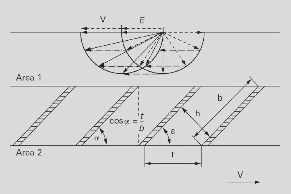
Image source: Pfeiffer Vacuum knowledge base Figure 4.22
| Pump type | Advantages | Limitations | Needs a backing pump? |
|---|---|---|---|
| Oil diffusion pump | High pumping speed, low cost | Needs cooling water and a backing pump; bulky, energy-hungry; oil-vapour backstreaming contaminates the film | Yes (mechanical pump + Roots pump) |
| Turbomolecular pump | Oil-free, high ultimate vacuum, stable pumping speed — the current mainstream in optical coating | Low pumping speed for light gases such as H2 and He; relatively costly | Yes (usually with a dry backing pump) |
| Cryopump Cryopump |
Inherently oil-free and cleanest; strongest at pumping water vapour and CO2, reaching ultra-high vacuum | Cannot run continuously and must be regenerated periodically; single-unit speed limited by cold-head area; high refrigeration and maintenance cost | Mandatory. Before start-up a backing pump must pre-pump below 5 × 10⁻² mbar; during regeneration the backing pump must also remove released gas |
Source: Yuanhuai Tech, Shanghai Kante Vacuum, ULVAC cryopump technical material
Selection conclusion:
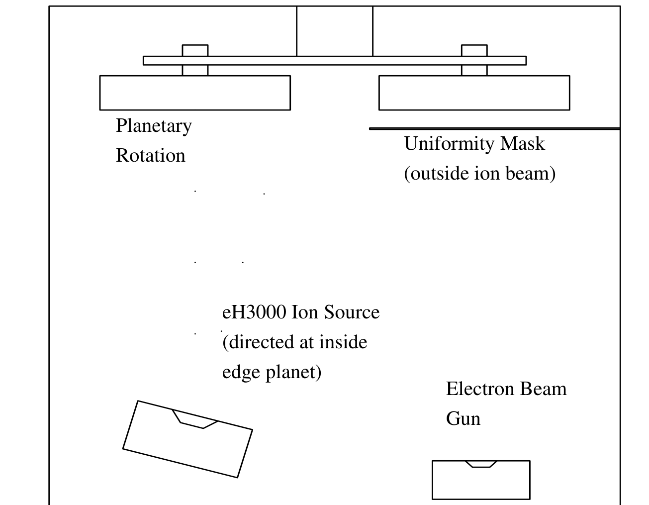
Image source: Vacuum Innovations LLC technical note AN-01 Shift-Free Optical Coatings
Select pumps according to the equipment maker’s standard configuration for the coater; do not change the main pump on your own. For continuous production and overall cost-effectiveness, a turbomolecular pump plus a dry backing pump remains the safer choice; where cleanliness demand is extreme and production is batchwise, a cryopump may be considered.
6. Laser-Induced Damage Threshold: 1064 nm High-Power Coating Parameters and Practice
Everything above addresses ‘optical performance’, but for a laser component what truly decides whether it can be used on a machine is the laser-induced damage threshold (LIDT) — the laser fluence the component withstands without damage.
6.1 Physical mechanisms of LIDT
The damage mechanism changes with laser type, and this determines the logic of material selection:
- Pulsed lasers: dominated by nonlinear and multiphoton absorption. The material band gap (strongly correlated with refractive index) decides whether electrons can be excited across it, so both substrate and film material must enter the design.
- Continuous-wave lasers: dominated by thermal effects from linear absorption, making thermal conductivity the key material property.
- Common factor: even with correct material and design, defect-initiated nodules intensify the local electric field and make the real damage threshold lower than the intrinsic material value — which is why defect control matters so much for high-power lasers.
6.2 Band gap versus LIDT
Under pulsed lasers, this set of data explains why film-material choices for high-power laser coatings are converging:
| Film material | Band gap (eV) | Refractive index n | LIDT (J/cm²) | Notes |
|---|---|---|---|---|
| Ta2O5 | 4.1 | 2.1 | 2.2 | Highest refractive index, but small band gap and lowest damage threshold |
| HfO2 | 5.3 | 1.9 | 3.4 | Wide band gap, the mainstream choice for high-power laser films |
| Al2O3 | 6.5 | 1.65 | 4.2 | Can also serve as a protective layer |
| SiO2 | 7.5 | 1.46 | 6.3 | First choice on the low-index side, with the widest band gap |
Source: Excelitas white paper on high-energy laser optics
Wider band gap and higher LIDT mean lower refractive index — an inherent contradiction. Design wants high reflectance and thus high index contrast, but high-index materials happen to have low damage thresholds. Multilayer design is precisely about finding the balance in this contradiction.
6.3 Reference performance of 1064 nm high-power films
| Wavelength | HR (20 ns pulse) | AR (20 ns pulse) | Continuous wave (CW) | Notes |
|---|---|---|---|---|
| 1064 nm | 50 J/cm² | 30 J/cm² | 20 MW/cm² | Mainstream fibre lasers |
| 532 nm | 30 J/cm² | 15 J/cm² | — | Frequency-doubled / green lasers |
| 355 nm | 10 J/cm² | 5 J/cm² | — | Third-harmonic UV |
Source: Excelitas published LIDT performance benchmarks (baseline performance expectations, not limits)
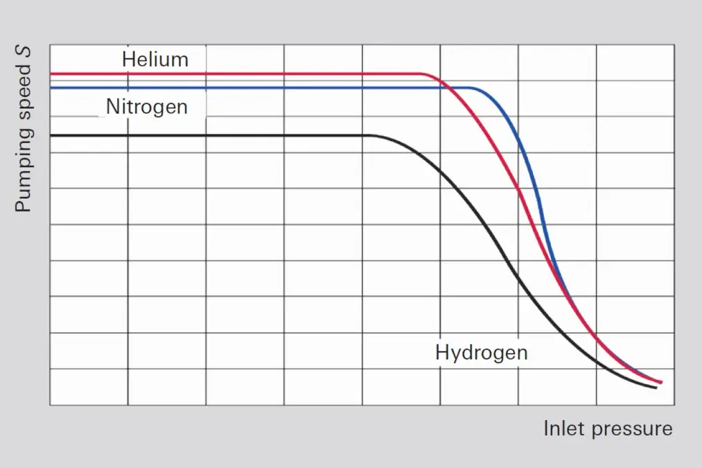
Image source: Pfeiffer Vacuum knowledge base Figure 4.25
As a higher-end reference: in the 2018–2019 1064 nm nanosecond-pulse high-reflector damage competition, the best of 41 entries was electron-beam-deposited HfO2/SiO2 high-reflection film, measured at 82 J/cm² by raster scan and 100 J/cm² by the ISO ‘no damage’ criterion. Comparable Ta2O5-based designs were mostly in the 13–19 J/cm² range. This is the empirical basis for HfO2 gradually replacing Ta2O5 in high-power lasers.
Source: public report of the 2018–2019 1064 nm thin-film damage competition
6.4 How defects eat the damage threshold
A 10 μm defect on a typical HfO2/SiO2 high-reflection film under 20 ns @1064 nm illumination has about a 50% chance of initiating damage at 50 J/cm2. Two practical conclusions follow:
- LIDT is not an ‘absolute value’ but a statistic. Defects are sparsely distributed, so test results are inherently probabilistic. Demanding ‘absolutely no damage’ is unrealistic in engineering; the probability can only be lowered by improving surface quality, at rising cost.
- Always ask about the test method and criterion when purchasing. Raster scan, ‘No damage’ and ‘Damage initiation’ criteria can give figures differing several-fold. Asking only ‘what is your LIDT’ without the criterion is the same as not asking.
A further engineering clue: if first damage in a batch occurs at scattered, irregular positions at the same fluence, it usually points to chamber cleanliness or incoming surface quality; if damage always appears at fixed positions, it is more likely substrate sub-surface damage (lapping microcracks) revealed by coating heat, and must be traced to the incoming substrate.
7. Quick Selection Guide: Working Back from Application to Film and Process
This table gives a ‘requirements-backwards’ route that can be followed directly when enquiring and selecting:
| Application | Film type | Key specifications | Process preference | Must confirm |
|---|---|---|---|---|
| Fibre laser cavity mirror | HR high reflection | 1064 nm reflectance > 99.9%; LIDT | E-beam / IBS / ion plating, HIL materials | LIDT criterion, mirror deformation |
| Laser output window | AR anti-reflection | Residual reflectance; incidence-angle range | IAD / magnetron sputtering | Whether double-sided AR design is needed |
| Field lens (F-Theta lens) | AR anti-reflection | Transmittance at working distance; broadband need | IAD / magnetron sputtering | Working-band span, field angle |
| Protective window | AR anti-reflection | Abrasion resistance, cleanability | Protective-layer design | Whether it withstands plasma spatter |
| Beam expander / beam splitter | BS beam splitting | R:T ratio; angular separation | IAD / IBS | Effect of incidence angle on split ratio |
| Polarising components | PBS | Extinction ratio; working band | Multilayer dielectric film | Bandwidth, extinction-ratio consistency |
| UV optics | AR / HR | UV transmission range; LIDT | Fluoride film materials preferred | UV ageing stability |
7.1 Five must-ask items when purchasing and enquiring
These are the points most often missed in practice, and the costliest to miss:
- Which criterion was LIDT measured with? Raster scan / No damage / Damage initiation can differ several-fold.
- What is the film-material scheme? For high power, confirm whether HfO2 is used rather than Ta2O5.
- Deposition process and density specification? IAD or IBS, and what equivalent temperature.
- Film tolerance commitment? Centre-wavelength drift and batch-to-batch consistency range of transmittance specifications.
- Is tolerance analysis and yield data available? This directly shows whether the supplier ‘can calculate’ or ‘can manufacture’.
8. Common Misconceptions: Six Widespread False Claims
The six below circulate widely in industry literature, supplier introductions and even some technical documents, but are all wrong. The first three are the most common.
Misconception 1: The higher the vacuum, the better.
Not quite. Base pressure indeed cannot be too high (i.e. too poor), but working pressure must stay within the process window — too low a pressure makes the plasma hard to sustain and the film actually porous. The two must be discussed separately.
Misconception 2: A cryopump needs no backing pump.
Wrong. Before starting, a cryopump (cryogenic pump) must be pre-pumped by a backing pump below 5 × 10⁻² mbar, otherwise the cold head cannot trap gas effectively; gas released on each regeneration must also be removed by the backing pump or the pump cannot reset. The ‘backing-pump-free’ claim is marketing for certain specific models, not a general fact.
Misconception 3: List thermal evaporation, sputtering and ion plating as ‘three heating methods’.
Wrong classification dimension. Evaporation and sputtering are two film-forming mechanisms (the first by melting and vaporising, the second by ion bombardment), while ion plating is a plasma-enhancement means layered on evaporation — an enhanced process, not an independent category. Moreover ‘sputtering heats’ is itself invalid — sputtering is a physical bombardment process of momentum transfer, not heating.
Misconception 4: A λ/4 film thickness is always anti-reflective.
λ/4 satisfies only the phase condition. True anti-reflection also needs the film index close to √(n0·ns) and the phase-jump premise to hold. Phase and amplitude conditions are both indispensable — which is why a single-layer film has a reflectance floor.
Misconception 5: A film design from software can go straight into production.
It cannot. Design results must be verified by tolerance-sensitivity and yield analysis, accounting for deviations of measured n/k from design values. A V-type four-layer AR film with ±1% systematic thickness error drops peak transmittance from 99.8% to 99.3%–99.5%; a 532 nm narrowband filter with 1% random error can drop from 90% to below 85%.
Misconception 6: Higher LIDT means a better film — just compare the number.
LIDT is a statistic and depends strongly on test criterion and method. Defect size, distribution and surface cleanliness all affect the result significantly. Two batches both quoted at 30 J/cm² can measure very differently. The right approach is to confirm the criterion, test method and sample-batch consistency together.
Reference sources
- RP Photonics Encyclopedia — Dielectric Coatings / Thin-Film Interference, rp-photonics.com
- Excelitas Technologies — White Paper on High Energy Laser Optics (including band gap–n–LIDT relationships and band-specific LIDT benchmarks)
- Public report of the 2018–2019 1064 nm nanosecond-pulse high-reflector thin-film damage competition (OSTI / Spica Technologies testing)
- TFCalc official feature list — Hulinks / Guangyan Tech, hulinks.co.jp
- GB/T 3224 ‘Vacuum Technology Terms’, China Standard Press; vacuum-region divisions also refer to public technical material from mainstream domestic vacuum-equipment makers
- Edmund Optics — Anti-Reflection Coatings application guide
- Public technical material from Ouguang Tech, Zhongce Opto-tech, Tianzhuo New Materials and Yuanhuai Vacuum (defect causes, vacuum grading and pump selection)
— Compiled by the Changsha Soar Laser technical team; parameters are typical engineering values. Actual selection should combine specific conditions, process windows and measured data, or contact the Soar Laser technical team for selection advice. —
Leave a Reply