


Description
Opto Diode AXUV100G 100 mm2 Windowless Si Photodiode for EUV / Soft X-Ray / Electron Detection
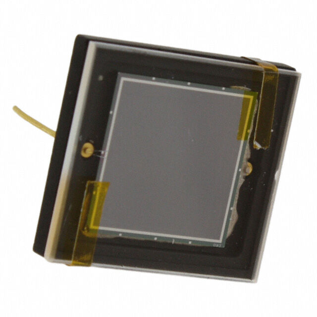
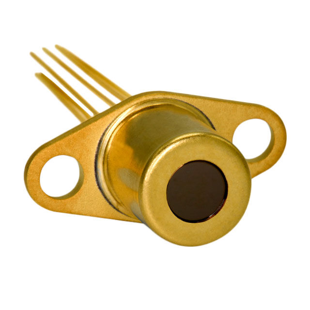
Opto Diode AXUV100G is a 100 mm² (10 mm × 10 mm) windowless silicon photodiode, the electron-detection version of the AXUV series, shipped with a temporary protective cap. Its spectral response covers soft X-rays and extreme ultraviolet (1–200 nm) and extends through UV–visible–near-IR (to 1100 nm), with a stable response to electrons of 100 eV–100 keV energy. Typical responsivity 0.08 A/W (@254 nm, 0.07–0.09 A/W), shunt resistance ≥20 MΩ, dark current approx. 2 nA, junction capacitance 5–15 nF (VR = 0 V), rise time ≤10 μs — suited to synchrotron beamline diagnostics, EUV source monitoring, electron-beam current measurement and VUV spectroscopy. The tax-inclusive price is shown in the price box on this page (13% VAT included).
Product Overview
The core value of the AXUV100G lies in two points: large area and windowless direct illumination. The active area is 10 mm × 10 mm (100 mm²) — large for an EUV / soft-X-ray detector, so divergent or wide parallel beams do not demand precise spot alignment, and the device can even give a rough assessment of beam cross-section uniformity. There is no window: photons enter the oxide-passivated silicon junction directly, avoiding the strong absorption and radiation-induced colour-centre problems of window materials in the 1–200 nm band — light in this band has absorption lengths of only microns to millimetres in air, so any window would cause severe attenuation.
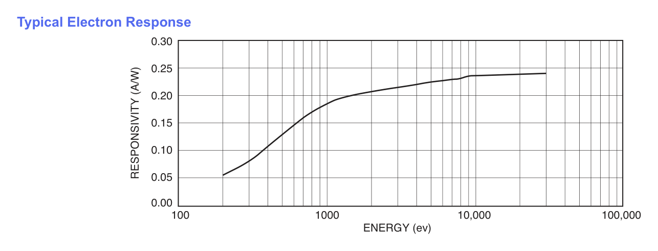
Compared with the Opto Diode SXUV100 of the same area and package, the AXUV100G is positioned as a general-purpose high-energy photon and electron detector: the datasheet title page marks it “Ideal for Electron Detection” and gives a typical electron response curve for 100 eV–100 keV; the shunt-resistance figure is higher (≥20 MΩ vs ≥10 MΩ for SXUV100), helping low-noise DC measurement. The trade-off is speed: the 100 mm² junction brings 5–15 nF of capacitance and a rise-time specification of 10 μs (RL = 50 Ω, VR = 0 V), so it targets DC photocurrent, pulse energy (μs scale and above) and integrating measurements, not nanosecond pulse-form recovery. For faster response choose a small-area model or re-check bandwidth within the series.
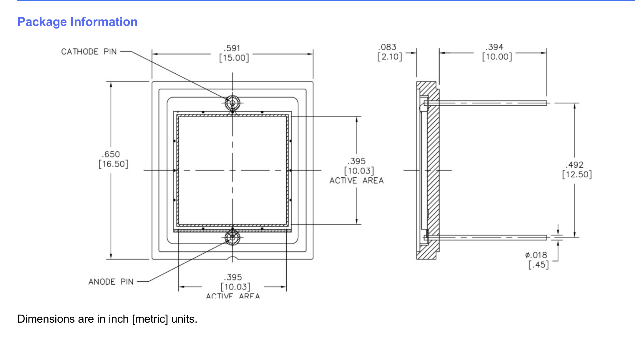
The package is a 16.50 × 15.00 × 2.10 mm square structure with a 10.03 mm square active region, two leads (cathode / anode) on 12.50 mm centres, Ø0.45 mm, suitable for through-hole soldering or mounting on flanges, PCBs and vacuum-chamber feedthroughs. The unit ships with a temporary protective cap for the chip surface and wire bonds, which must be removed per the manufacturer’s application note “Handling Precautions for AXUV, SXUV, and UVG Detectors” before use. AXUV100G is made by Opto Diode Corp (a US ITW company) and supplied original by Soar Laser; parameters on this page come from the manufacturer datasheet (Revision 2022-12-17) cross-checked against public materials (checked 2026-11-04).
Key Features
- Large 100 mm² area (10 mm × 10 mm): strong light collection, insensitive to spot alignment and beam divergence — suited to divergent EUV sources and wide beams
- Windowless oxide-passivated structure: no window absorption or radiation colouring in 1–200 nm; photons enter the silicon junction directly
- Soft X-ray / EUV to near-IR broadband response: 1–200 nm as the primary band, usable response also in 200–1100 nm (see curves)
- Optimised for electron detection: typical response 0.05–0.24 A/W for 100 eV–100 keV electrons, suited to electron beam current and energy monitoring
- High shunt resistance ≥20 MΩ (VB = ±10 mV): low noise in zero-bias photovoltaic mode, stable zero point for weak signals
- Low dark current: approx. 2 nA typical, suited to DC photocurrent measurement at nA levels and above; for lower light levels use modulation + lock-in or a small-area low-dark-current model
- Zero-bias or reverse-bias operation: reverse breakdown 5–10 V; reverse bias lowers junction capacitance and shortens rise time, but dark current rises — weigh the SNR
- Temporary protective cap as shipped: protects the active area and wire bonds during transport and assembly
- Vacuum compatible: −10 to 40 °C in ambient; −20 to 80 °C in nitrogen or vacuum — can be mounted directly in vacuum chambers
- RoHS compliant, MSL 1 (unlimited), ECCN EAR99 — easy export and production introduction
Technical Specifications
| Parameter | Value |
|---|---|
| Manufacturer | Opto Diode Corp (a US ITW company) |
| Manufacturer part number (MPN) | AXUV100G |
| Product type | Silicon photodiode (windowless, electron-detection type) |
| Series | AXUV |
| Spectral range | 1 nm–1100 nm (primary 1–200 nm; responsivity spec measured at 254 nm) |
| Electron detection energy range | 100 eV–100 keV (typical response curve) |
| Active area | 100 mm² (10 mm × 10 mm) |
| Responsivity | 0.07 / 0.08 / 0.09 A/W (min / typ / max, @254 nm, VR = 0 V) |
| Shunt resistance | ≥20 MΩ (VB = ±10 mV) |
| Reverse breakdown voltage | 5 V (min) to 10 V (max), IR = 1 μA |
| Junction capacitance | 5 nF (typ) to 15 nF (max), VR = 0 V |
| Rise time | ≤10 μs (VR = 0 V, RL = 50 Ω) |
| Dark current | Approx. 2 nA (typical) |
| Operating temperature — ambient | −10 °C to 40 °C |
| Operating temperature — nitrogen or vacuum | −20 °C to 80 °C |
| Lead soldering temperature | 260 °C, 2.03 mm (0.080 in) from the body, ≤10 s |
| Package | Square through-hole package, 2 leads (anode / cathode), temporary protective cap as shipped |
| Outline dimensions | 16.50 mm × 15.00 mm × 2.10 mm (.650 × .591 × .083 in) |
| Active area dimensions | 10.03 mm × 10.03 mm (.395 × .395 in) |
| Lead spacing / diameter | 12.50 mm / Ø0.45 mm (.492 / Ø.018 in) |
| Mounting | Through-hole (THT) |
| Incident illumination | Windowless direct illumination (the incident surface is the silicon chip surface) |
| Packaging | Bulk, manufacturer standard package of 1 unit |
| Status | Active |
| Lead time | Made to order; factory standard lead time approx. 18 weeks (subject to our confirmation) |
| RoHS | RoHS compliant (RoHS3) |
| MSL | 1 (unlimited) |
| ECCN | EAR99 |
| HTSUS | 8541.49.1050 |
| Note: values are nominal figures from the Opto Diode official datasheet (Revision December 17, 2022); the typical dark current is taken from public manufacturer materials (2026-11-04). Responsivity, junction capacitance and dark current vary with wavelength, bias and temperature — calibrate under actual conditions before quantitative measurement. |
Package Dimensions & Characteristic Curves
- Figure 1 — AXUV100G outline & mounting dimensions: 16.50 × 15.00 mm outline, 2.10 mm thick, 10.03 mm square active area, 12.50 mm lead spacing; cathode/anode positions per the drawing (units inch [mm]; source: Opto Diode official datasheet)
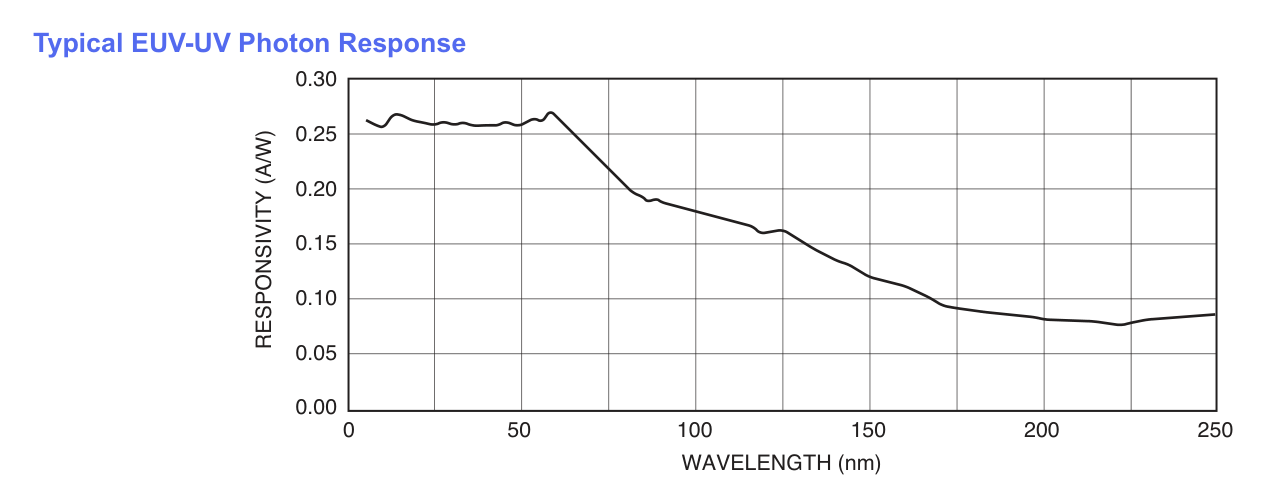
- Figure 2 — Typical EUV–UV photon responsivity: about 0.26 A/W over the 0–60 nm plateau, falling with wavelength — about 0.12 A/W at 150 nm and 0.08 A/W at 250 nm (source: Opto Diode official datasheet)
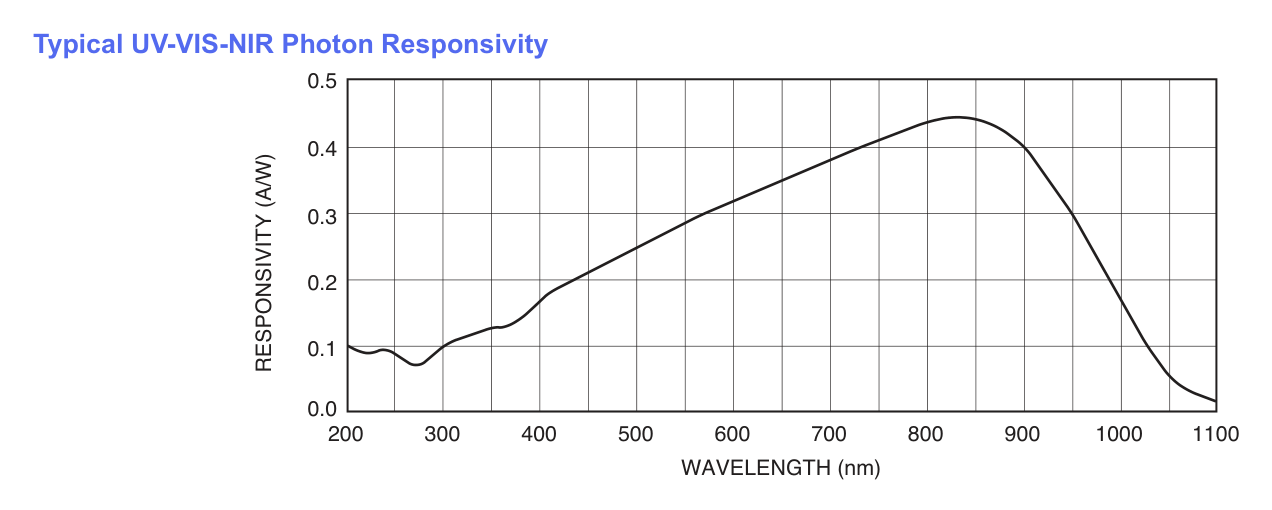
- Figure 3 — Typical UV–VIS–NIR responsivity: rising from 200 nm, peaking near 0.44 A/W around 850 nm, with a rapid cut-off after 1050 nm (source: Opto Diode official datasheet)
- Figure 4 — Typical electron response: about 0.05 A/W at 100 eV, 0.19 A/W at 1 keV, about 0.24 A/W above 10 keV (source: Opto Diode official datasheet)
Q: What is the AXUV100G, and how does it differ from ordinary silicon photodiodes?
A: AXUV100G is the 100 mm² windowless silicon photodiode of the Opto Diode AXUV series, designed for soft X-rays, extreme ultraviolet (EUV) and electron detection. Three key differences: (1) windowless structure — photons at 1–200 nm reach the silicon junction without passing a window, avoiding window absorption and radiation colouring; (2) large 10 mm × 10 mm area — strong light collection for divergent sources and wide beams; (3) an oxide-passivated silicon junction with high shunt resistance (≥20 MΩ) for low noise and a stable zero point on weak signals. Ordinary windowed silicon PIN diodes have little useful response below 200 nm.
Q: How do I choose between AXUV100G and SXUV100?
A: Same area, outline and package; the difference is process positioning. AXUV100G is the general-purpose version, marked by the manufacturer as ideal for electron detection with a 100 eV–100 keV electron response curve and higher shunt resistance (≥20 MΩ); SXUV100 is the radiation-hardened version with passivation for long-term exposure to high-power-density EUV/UV, with more stable post-irradiation response. For electron-beam measurement, soft-X-ray/VUV spectroscopy and general EUV energy measurement choose AXUV100G; for long-term on-line monitoring on EUV lithography sources or synchrotron beamlines, SXUV100 is the safer choice.
Q: Which wavelengths can it measure? Does it work for both 254 nm UV and 13.5 nm EUV?
A: Both, but responsivity varies greatly. Soft X-ray to EUV (0–60 nm) is typically about 0.26 A/W — the highest part of the spectrum; about 0.12 A/W at 150 nm and 0.08 A/W at 250 nm; response rises again into visible–near-IR, about 0.44 A/W near 850 nm with rapid cut-off after 1050 nm. 254 nm is exactly the manufacturer’s responsivity test point (0.08 A/W, 0.07–0.09 A/W). Note that 1–200 nm light is strongly absorbed in air — the beam path must be evacuated or purged with inert gas; this is a beam-path requirement, not a device limitation.
Q: Isn’t a 100 mm² large area too slow?
A: Yes. Junction capacitance is 5–15 nF at 0 V with a rise-time specification of ≤10 μs (RL = 50 Ω, VR = 0 V), so it suits DC photocurrent, pulse energy at μs scale and above, and integrating measurements — not nanosecond waveform recovery. For more bandwidth, apply reverse bias (breakdown 5–10 V; in practice keep within 5 V) to reduce capacitance, or choose a small-area model; reverse bias raises dark current, so re-check the SNR.
Q: How is electron detection connected, and how are responses converted?
A: Electrons strike the bare silicon surface directly, creating electron–hole pairs in the depletion region that form the current — no scintillator or phosphor screen needed. Typical response: about 0.05 A/W at 100 eV, 0.19 A/W at 1 keV, about 0.24 A/W above 10 keV. In practice charge conversion is often used: producing one electron–hole pair in silicon takes about 3.6 eV, so a 10 keV electron generates roughly 2,800 carriers. Operate the device in a vacuum chamber, keep the electron-beam power density within the chip’s heat dissipation, and add a beam-limiting aperture if necessary.
Q: Must the protective cap be removed? What about cleaning and installation?
A: The temporary cap shipped with the unit protects the chip and wire bonds and must be removed before use per the application note “Handling Precautions for AXUV, SXUV, and UVG Detectors”. The device is ESD-sensitive: wear a grounded wrist strap and work on a grounded surface; never touch or wipe the active area and do not soak it in solvents, to avoid damaging the passivation layer and bond wires; when soldering keep lead temperature below 260 °C, at least 2.03 mm from the body and no longer than 10 s per operation. Long-term operation above 40 °C accelerates growth of the surface oxide, irreversibly reducing responsivity below 150 nm.
Q: Is it in stock? What is the lead time? What does the price include?
A: AXUV100G is a make-to-order item with a factory standard lead time of about 18 weeks — for urgent needs check in-transit stock with us first. The tax-inclusive price shown on this page (13% VAT included) is our RMB selling price, minimum order 1 unit; volume purchasing, companion transimpedance amplifiers, bias sources or vacuum-flange mounting hardware can be quoted separately.
Ordering Information
Ordering model: AXUV100G (manufacturer: Opto Diode Corp). The series is divided into multiple models by active area and purpose (e.g. AXUV20HS1, AXUV63HS1, AXUV100, SXUV100), with markedly different area, capacitance and responsivity — confirm by spot size, bandwidth and irradiation conditions when selecting; they are not directly interchangeable.
For companion transimpedance amplifiers, bias supplies, vacuum feedthrough flanges, or factory-screened / calibrated versions, contact our engineers for a solution and quotation.
Disclaimer
Parameters, curves and dimension data on this page are compiled from the Opto Diode official datasheet (Revision December 17, 2022) and public product materials (collected 2026-11-04) and cross-checked; actual product parameters, appearance and packaging are subject to the manufacturer’s shipment, and specifications may change without notice.
This product is an ESD-sensitive device with an exposed windowless active area — take ESD and cleanliness precautions when handling; bias voltages, optical power density, electron-beam power or temperature beyond specification may permanently damage the device, and such losses are not covered by warranty.
The product is intended for lawful scientific research, industrial and similar uses only. Opto Diode is a trademark of its respective owner and is used here for product description only.
Reviews
There are no reviews yet.