


What Is a Photodiode? The Most Fundamental Light-Detection Device
I. Core Concept: What Is a Photodiode?
When it comes to photodiodes, many people’s first reaction may be “that sounds very specialised.” But if you know something about lasers, you know the photodiode is a very central, very fundamental device in the laser field.
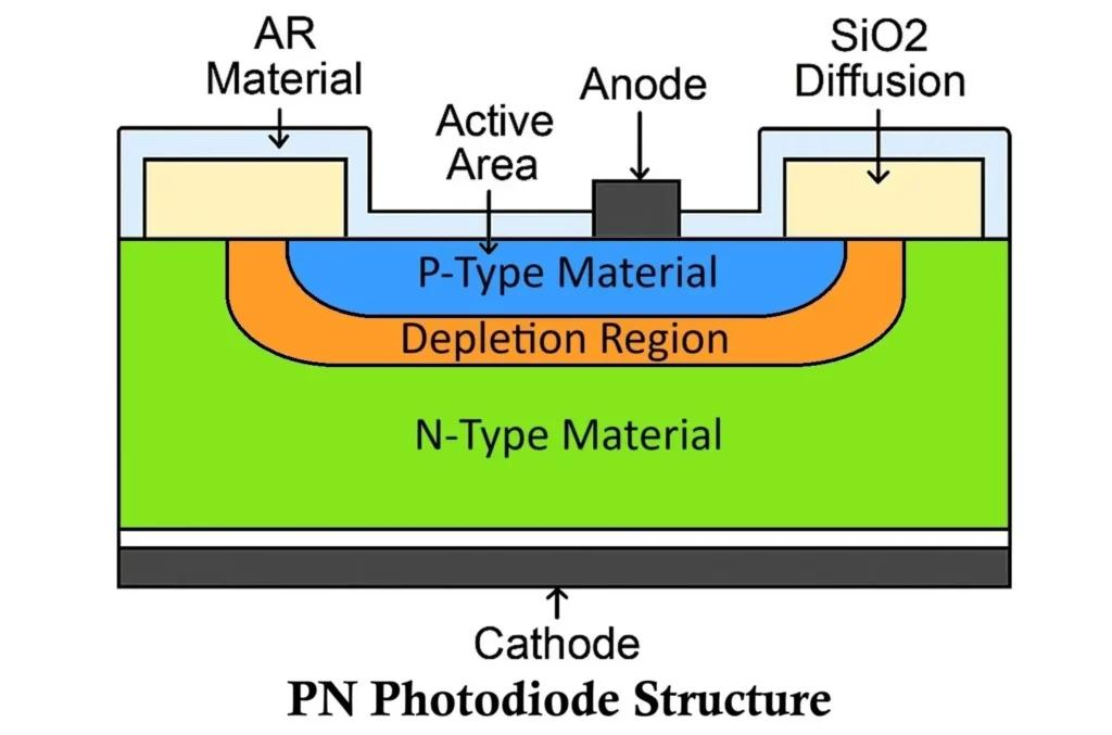
A photodiode (PD) is the most basic and most widely used semiconductor photodetector. It is essentially a semiconductor diode with a p-n junction or p-i-n structure that converts incident photons directly into a current signal. In the laser and optoelectronics industries, the photodiode is like the core probe of an “optical multimeter” — it appears in power meters, optical receivers, optical sensors and almost every such device.
Unlike an ordinary diode, a photodiode is designed to let as many photons as possible enter the depletion region and be effectively absorbed, generating as many photocarriers as possible. It is compact, fast and linear — the undisputed “workhorse” device of optoelectronics.
Some may ask, why dedicate a whole article to photodiodes? Because almost every light-detection scenario — from the simplest optical power measurement to the most complex high-speed optical communication — depends on photodiodes. Understanding their principles, parameters and selection methods is the first step to using photodetection technology well.
II. How It Works: How a Photodiode Is Realised
To understand how a photodiode works, it can be broken down into several key steps. Let’s go step by step:
Photon Absorption and Carrier Generation
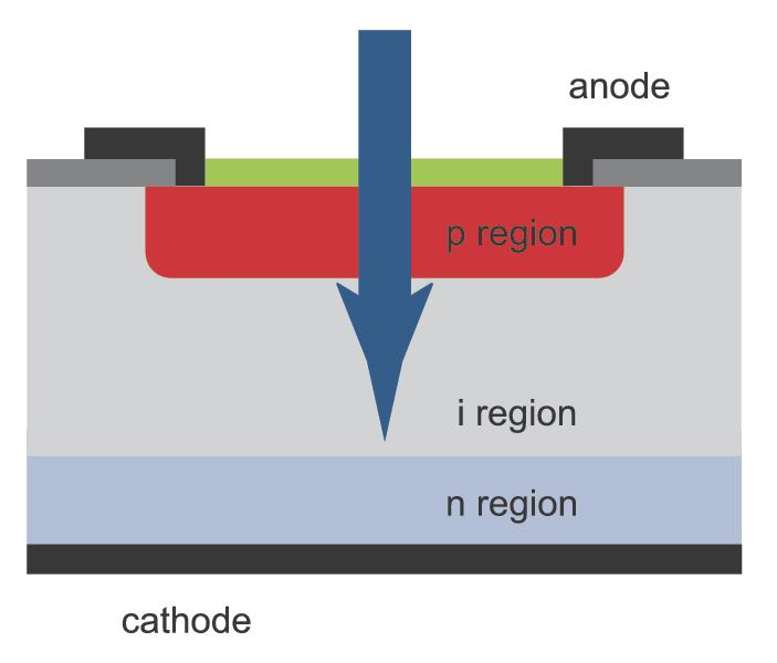
When photons enter the semiconductor material of a photodiode, if the photon energy exceeds the material’s bandgap, electrons in the valence band are excited to the conduction band, generating an electron-hole pair. This process occurs mainly in and near the depletion region (or intrinsic layer).
Carrier Transport and Photocurrent Formation
There is a built-in electric field at the p-n junction (aided by an external field under reverse bias). The electron-hole pairs generated in the depletion region are rapidly separated by the field — electrons drift toward the n region and holes toward the p region — forming a measurable photocurrent in the external circuit. This photocurrent is essentially proportional to the incident optical power.
Signal Readout Mechanisms
Depending on the operating mode, the photocurrent can be read in different ways:
Photovoltaic mode (zero bias, Photovoltaic Mode): with no reverse bias, the photodiode acts as a photovoltaic cell, outputting a photovoltage or photocurrent. If an op-amp holds the voltage across the diode at zero (short-circuit mode), noise is low and linearity is good, but response is slower (large junction capacitance). Commonly used in precision optical power measurement and other situations not demanding speed but requiring strict linearity and low noise (RP Photonics Encyclopedia – Photodiodes).
Photoconductive mode (reverse bias, Photoconductive Mode): with reverse bias applied, the depletion region widens and junction capacitance decreases, giving faster response and a larger dynamic range. But reverse bias introduces dark current and relatively higher noise. This is the mainstream mode for high-speed applications such as optical communication and pulse measurement.
| Comparison Item | Photovoltaic Mode (Zero Bias) | Photoconductive Mode (Reverse Bias) |
|---|---|---|
| Bias Voltage | 0 V (zero bias) | Reverse bias (a few V to tens of V) |
| Dark Current | Very low (near zero) | Higher (increases with reverse bias) |
| Noise Level | Low | Relatively higher |
| Linearity | Good (very linear in short-circuit mode) | Good (over 6 orders of magnitude) |
| Response Speed | Slow (large junction capacitance) | Fast (small junction capacitance, wide depletion region) |
| Dynamic Range | Narrower | Wide |
| Typical Applications | Precision optical power measurement, photometers, low-speed sensing | High-speed optical communication, pulse measurement, fast-response applications |
Common Structure: PIN Photodiode
The PIN (p-i-n) structure is the most commonly used and most classic photodiode design. It inserts a thick layer of intrinsic semiconductor (i-layer) between the p and n regions; the intrinsic layer is lightly doped or undoped semiconductor material with very high resistivity.
Advantages of the PIN structure:
- Wider depletion region: the i-layer is almost fully depleted, photon absorption occurs mainly in the i-layer, giving high quantum efficiency
- Smaller junction capacitance: the i-layer increases the distance between p and n regions, greatly reducing junction capacitance Cj and giving faster response
- Better linearity: carriers move mainly by drift, giving high speed and good linearity
Because it balances speed and efficiency, the PIN photodiode has become the most widely used photodetector structure, with bandwidth reaching tens of GHz.
Responsivity formula: the responsivity R of a photodiode (in A/W) relates to the quantum efficiency η as follows:
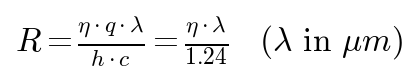
where q is the electron charge, h is Planck’s constant, c is the speed of light and λ is the wavelength. Thus responsivity is proportional to wavelength (within the material’s response range): longer wavelengths carry less energy per photon but produce the same number of electron-hole pairs (one photon generates one carrier pair), so the photocurrent per unit power is larger.
III. Key Parameters: Understanding Performance Metrics
To understand photodiodes, knowing concepts and principles is not enough — you must also understand their key parameters. The table below organises the core parameters clearly:
| Parameter | Meaning | Why It Matters |
|---|---|---|
| Responsivity (R) | The photocurrent produced per unit incident optical power, in A/W. Responsivity varies with wavelength, peaking at a certain wavelength. For example, silicon photodiodes peak around 900 nm at about 0.5–0.6 A/W. | The photocurrent per unit optical power, measuring conversion efficiency. Higher responsivity means a stronger output signal for the same input. Responsivity is closely wavelength-dependent and must be calibrated at the operating wavelength. |
| Quantum Efficiency (QE) | The fraction of incident photons actually converted into photoelectrons. High QE means photons are fully utilised, especially important in low-light detection. Quality PIN tubes can exceed 90% QE at the peak wavelength. | The fraction of incident photons generating photoelectrons, the fundamental metric of intrinsic detector sensitivity. Higher QE means better signal-to-noise in low light. |
| Response Speed / Bandwidth | The ability to follow changes in light intensity, mainly limited by two factors: carrier transit time in the depletion region (setting the upper speed limit) and the RC time constant from junction capacitance and load resistance. PIN tubes can reach tens of GHz. | The ability to track light-intensity changes, determined by junction capacitance and carrier transit time. High-speed communication and pulse measurement need high-bandwidth PDs. |
| Dark Current | With no illumination, the small leakage current that still exists in a photodiode under reverse bias. Dark current is an important noise source, especially significant in low-light detection. It grows exponentially with temperature. | The leakage current under reverse bias with no light, a source of noise. Lower dark current means better low-light detection. PIN types usually have very small dark current. Dark current is exponentially related to temperature — it roughly doubles per 7°C for silicon and per 10°C for InGaAs, depending on material and process [(RF Essentials – Dark Current)](https://rfessentials.com/resources/rf-glossary/dark-current/). |
| Noise-Equivalent Power (NEP) | The smallest optical signal a detector can resolve, usually expressed in W per √Hz. Smaller NEP means a more sensitive detector. It combines shot noise, thermal noise and dark-current noise. | Measures the detection-sensitivity floor of a PD; smaller NEP means more sensitive. It is the incident optical power at a signal-to-noise ratio of 1, reflecting the detector’s fundamental detection capability. |
| Spectral Response Range | Which wavelengths a photodiode responds to. Ordinary silicon tubes cover about 200–1100 nm (UV-enhanced types extend to 190 nm), InGaAs about 900–1700 nm, germanium about 800–1800 nm. The material bandgap determines the long-wavelength limit. | Determined by the semiconductor bandgap; silicon covers UV to ~1100 nm, InGaAs 900–1700 nm. The operating wavelength must be within the response range. Note that the UV band (<200 nm) requires UV-enhanced types or special window materials. |
| Linear Dynamic Range | The power range over which output photocurrent remains linear with incident optical power. The linear range of photodiodes is very wide, typically 6–8 orders of magnitude. | The power range over which output photocurrent stays linear with incident power. Beyond it responsivity drops and measurement distorts. |
| Photosensitive Area | The size of the effective light-sensitive region. Small-area tubes are fast with low junction capacitance; large-area tubes receive more optical power but are slower. | The size of the photosensitive region. Large areas couple light more easily but have high junction capacitance, slow response and high dark current. Small areas are fast but demand precise alignment. |
IV. Main Types: What Kinds of Photodiodes Exist?
Photodiodes can be classified in many ways; different dimensions help us understand their characteristics from different angles. The following introduces them by common classification approaches:
By Semiconductor Material
#### Silicon photodiodes (Si PD)
The most common type; ordinary silicon tubes cover about 200–1100 nm, UV-enhanced types extend to 190 nm, low cost and balanced performance, with very high quantum efficiency in visible and near-IR (peaks up to 80–90%).
#### InGaAs photodiodes
Mainly cover the near-IR band (~900–1700 nm), the standard choice for optical communication bands (1310 nm, 1550 nm). Large-area InGaAs detectors are relatively expensive.
#### Germanium photodiodes (Ge PD)
Cover about 800–1800 nm and can be used at 1550 nm, but with larger dark current than InGaAs and slightly inferior performance.
#### Other materials
Such as GaN (UV detection) and InAsSb (mid-IR), used for special wavelength bands.
By Structure
#### PN-type photodiodes
The simplest structure with mediocre performance, now less commonly used.
#### PIN-type photodiodes
A p-intrinsic-n three-layer structure, fast with high quantum efficiency, the current mainstream.
#### Avalanche photodiodes (APD)
Operate at high reverse bias, using impact ionization for internal gain and higher sensitivity. See the avalanche photodiode entry.
#### Schottky photodiodes
A metal-semiconductor contact structure, extremely fast, usable in ultrahigh-speed scenarios such as terahertz communication.
By Package and Application
#### Free-space type
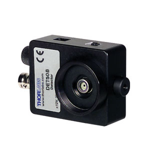
Used in free-space optical paths, with the photosensitive surface directly receiving incident light.
#### Fibre-coupled type
With a fibre pigtail or fibre adapter, convenient for connection to fibre systems.
#### Array type
Multiple photodiodes integrated on one chip, used for position sensing or parallel optical communication.
#### Integrated-amplification type
Integrates the photodiode with a transimpedance amplifier (TIA) for easier use.
Different photodiode types have their own strengths and weaknesses — there is no absolute “best,” only “most suitable.” Selection should consider your specific application comprehensively — response speed requirements, wavelength range, sensitivity needs, cost budget and other factors.
V. Applications: Where Are Photodiodes Used?
Photodiodes are among the most widely used devices in the laser and optoelectronics industries:
- Optical power measurement: the core sensing element of [optical power meters](https://www.soar-laser.cn/en/optical-power-meter-encyclopedia/), which, with integrating spheres and attenuators, cover an extremely wide power range from nanowatts to kilowatts.
- Fibre communication reception: the core device at the receiving end of high-speed optical communication systems, converting optical signals from fibre into electrical signals. 10G, 40G, 100G and higher-rate optical modules all rely on high-speed PIN tubes or APDs.
- Laser monitoring and control: power monitoring in lasers (MPD back-facet diode) and automatic power control (APC) loops that stabilize output power all rely on photodiodes.
- Optical sensing: serving as signal-conversion elements in displacement, vibration, temperature, gas-concentration and other optical sensors.
- Barcode scanning and laser rangefinding: used in industrial barcode readers, laser rangefinders and other equipment to detect reflected light signals.
- Biomedical detection: detecting weak light signals in flow cytometers, microplate readers, real-time fluorescence PCR and other equipment.
- Imaging applications: combined with scanning mechanisms for 1D/2D imaging, or serving as pixel units of image sensors.
VI. Common Misconceptions
Many people have plausible-sounding but wrong ideas about photodiodes. See if any of these misconceptions catch you out:
Misconception 1: The higher a photodiode’s responsivity, the more accurate the measurement
Responsivity is only a conversion-efficiency metric and has no direct relation to measurement accuracy. Accuracy depends on calibration precision, linearity, temperature stability, noise level and other factors. Moreover, responsivity varies greatly with wavelength, so the wavelength-correction factor must be set correctly in power-meter use, otherwise readings will have systematic bias. A precisely calibrated low-responsivity detector may measure more accurately than an uncalibrated high-responsivity one.
Misconception 2: Photocurrent is always proportional to optical power
A photodiode is very linear within a certain power range, but not always linear. At high optical power, excessive carrier concentration causes space-charge effects and field distortion, producing saturation — photocurrent grows more slowly or stops growing. In addition, voltage drop from series resistance causes nonlinearity. In practice, operation should stay within the linear region.
Misconception 3: Dark current is fixed and unchanging
Dark current is very temperature-sensitive. Silicon photodiode dark current roughly doubles per 7°C rise, InGaAs per 10°C (exact values vary by material and process). In high-temperature environments or low-light detection, increased dark current can significantly degrade noise performance. For low-level precision measurement, the temperature effect on dark current must be considered, using temperature control or compensation where needed. Reverse-bias magnitude also affects dark current.
Misconception 4: The faster a photodiode responds, the better
Fast response usually comes at the cost of sensitivity and photosensitive area. High-speed tubes generally have small junction area and capacitance, but receive less optical power and have relatively more noise. For slow applications (such as average power measurement), a high-speed tube is not only unnecessary but may introduce more noise due to excessive bandwidth. Selection should match the actual signal bandwidth — sufficient bandwidth is enough.
VII. Recommended Reading
- [Avalanche photodiodes: high-sensitivity detectors with built-in gain](https://www.soar-laser.cn/en/apd-avalanche-photodiode-encyclopedia/)
- [Photomultiplier tubes: why they can detect single photons](https://www.soar-laser.cn/en/pmt-photomultiplier-tube-encyclopedia/)
- [Photodetector noise and signal-to-noise ratio](https://www.soar-laser.cn/en/photodetector-noise-snr-encyclopedia/)
- [Optical power meters: how to accurately measure laser power](https://www.soar-laser.cn/en/optical-power-meter-encyclopedia/)
References:
- RP Photonics Encyclopedia – [Photodiodes](https://www.rp-photonics.com/photodiodes.html)
- Hamamatsu Photonics – Photodiode Handbook
- Thorlabs – Biased Photodetectors Lab Facts [(Thorlabs China)](https://www.thorlabschina.cn/biased-photodetectors-lab-facts)
Leave a Reply