


What Thin-Film Deposition Techniques Exist? How Optical Coatings Are Made
Thin-film deposition technology is an important concept in the laser field, widely used in industrial manufacturing, scientific research and healthcare. This article systematically introduces the core concepts, working principles, key parameters, main types and typical applications of thin-film deposition, helping readers build a complete knowledge framework.
Table of Contents
- I. What Is Thin-Film Deposition? Clarifying the Core Concept
- II. How Does Thin-Film Deposition Work?
- III. Key Parameters: Understanding Performance Metrics
- IV. Main Types: What Kinds of Thin-Film Deposition Exist?
- V. Application Scenarios: Where Is Thin-Film Deposition Used?
- VI. Common Misconceptions: Pitfalls to Avoid
I. Core Concept: What Is Thin-Film Deposition?
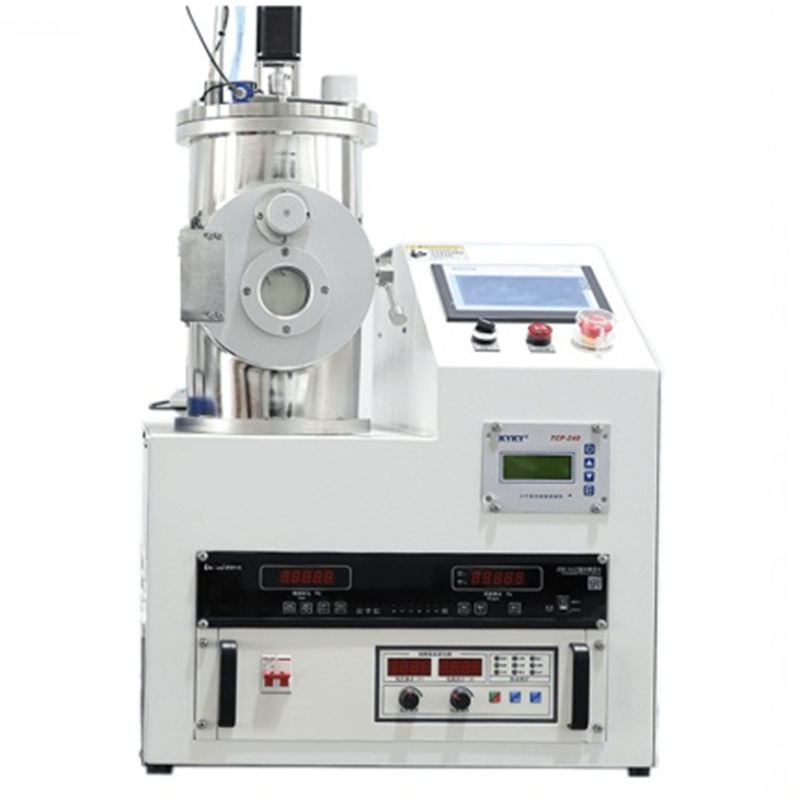
Thin-film deposition is the process of “coating” coating materials onto an optical substrate surface layer by layer in extremely thin form. If coating design is the “recipe,” then deposition technology is the “kitchen and cooking skill” – the same design can produce films of wildly different quality with different deposition processes. Optical thin-film deposition is usually performed in a high-vacuum environment, because dust and gas molecules in air seriously affect film quality. The core goals of deposition technology are: precisely controlling each layer’s thickness (often to sub-nanometre accuracy), ensuring uniform and dense films with strong adhesion, accurate material composition and few defects. For laser applications, the deposition process also directly determines the coating’s laser damage threshold and environmental stability. Understanding the characteristics of different deposition processes is the key for salespeople to explain “why the same coating varies so much in price.”
II. How Does Thin-Film Deposition Work?
Different deposition techniques work on different principles, but essentially all turn the coating material into a vapor/plasma state and then let it condense into a thin film on the substrate surface. Thermal evaporation processes (such as e-beam evaporation and resistive evaporation) heat the material to melt and vaporize it; the vapor travels through the vacuum chamber to the cooler substrate and condenses into a film. These processes have relatively low energy and the resulting films often have columnar structure with low density. Sputtering processes (such as ion beam sputtering and magnetron sputtering) bomb a material target with high-energy ions, “knocking” target atoms loose; these sputtered atoms have high kinetic energy and form very dense films when they land on the substrate. Ion-assisted deposition (IAD) bombards the growing film with an ion beam during evaporation – like “pounding while coating” – to increase film density. Different processes input different energy, so the resulting film’s microstructure and performance differ.
💡 An analogy
Thin-film deposition is like stacking a cake on an optical component – each layer’s thickness must be precisely controlled (to sub-nanometre accuracy) and the material combination must be accurate, just as each cake layer’s flavor and thickness must be exact. Different deposition processes are like different cooking methods, producing wildly different “taste” (film quality).
III. Key Parameters: Understanding Performance Metrics
Understanding thin-film deposition requires mastering the following key parameters, which directly determine product performance and applicable scenarios:
| Parameter name | Meaning | Why it matters |
|---|---|---|
| Film thickness control accuracy | The ability to control each layer’s thickness error, usually expressed as a percentage; higher accuracy means more accurate spectral performance | Determines whether the coating achieves designed spectral performance; accuracy usually must be better than 1%, otherwise transmission/reflection spectra deviate from target |
| Film density | The ratio of the film’s actual density to bulk material density, affecting refractive index, environmental stability and damage threshold | Affects refractive index, environmental stability and laser damage threshold; dense films absorb less water and perform more stably |
| Uniformity | Thickness consistency across the entire substrate surface, especially important for large-size components | Thickness consistency over the whole substrate, especially important for large-aperture components and mass production |
| Deposition rate | How much thickness can be coated per unit time, affecting throughput and cost | Affects production efficiency and cost, but excessive rate often sacrifices film quality and accuracy |
| Adhesion | The bond strength between film and substrate and between film layers; poor films peel easily | The bond strength between film and substrate and between layers; poorly adhering films peel and fail easily |
| Surface roughness | How smooth the film surface is, affecting scattering loss | Affects scattering loss, especially critical for high-power lasers and low-loss applications |
The above parameters are interrelated and mutually constraining. Actual selection requires comprehensive trade-offs among performance, cost and reliability based on specific application needs.
For more product parameters or selection advice, please contact the Soar Laser technical team.
IV. Main Types: What Kinds of Thin-Film Deposition Exist?
There are many thin-film deposition techniques, each with its own features and suitable scenarios. The following are the most common optical coating deposition techniques:
E-beam Evaporation
Uses an electron beam to bombard material in a crucible to vaporize it – the most traditional and mature process. Equipment and running costs are low, suitable for mass production, but the film is relatively loose with density about 70%-90%, average environmental stability and medium damage threshold.
Ion-Assisted Deposition (IAD)
Adds ion-beam bombardment of the substrate on top of e-beam evaporation, improving film density and adhesion. Oxide film quality is good, refractive index closer to bulk material, significantly better environmental stability, but fluoride materials are easily decomposed by ion bombardment.
Ion Beam Sputtering (IBS)
Uses a high-energy ion beam to bombard a target, sputtering target atoms that deposit on the substrate. Film density is extremely high (near 100%), damage threshold high, repeatability good, but deposition rate is slow and cost high – suitable for high-precision, high-power applications.
Magnetron Sputtering
Uses a magnetic field to confine plasma, improving sputtering efficiency. Fast deposition rate, dense films, suitable for large-area uniform coating, widely used in industrial production. Can be divided into DC sputtering and RF sputtering.
Atomic Layer Deposition (ALD)
Alternating precursor gases deposit atomic-layer-thick films layer by layer. Extremely high thickness control accuracy (sub-angstrom), excellent uniformity and step coverage, but extremely slow deposition and high cost.
Plasma-Enhanced Chemical Vapor Deposition (PECVD)
Uses plasma to activate chemical reactions, depositing films at relatively low temperatures. Can deposit high-quality films at low temperature, suitable for temperature-sensitive substrates, but material choices are limited.
Different deposition processes each have advantages and disadvantages in film quality, cost, efficiency and applicable materials. Which process to choose requires comprehensive consideration of specific performance requirements, budget and output. Generally, for high-power laser applications demanding damage threshold and stability, ion beam sputtering is preferred; for cost-sensitive mass-production applications, e-beam evaporation and magnetron sputtering are more common.
V. Application Scenarios: Where Is Thin-Film Deposition Used?
Thin-film deposition has a very broad range of applications – from industrial manufacturing to healthcare, from communication networks to scientific research, nearly everywhere lasers are used. A brief look by field:
- Different deposition processes suit different applications. E-beam evaporation, because of low cost and wide material choice, is the mainstay of low-to-mid-end optical coatings – AR coatings on consumer electronics lenses, eyeglass lenses and ordinary optical components mostly use this process. Ion-assisted deposition (IAD) strikes a good balance between cost-effectiveness and performance, widely used in medium-requirement laser optics and industrial optics. Ion beam sputtering (IBS) is the first choice for high-end laser optics – femtosecond laser chirped mirrors, high-damage-threshold cavity mirrors, ultra-narrowband filters and ultra-low-loss high-reflection mirrors demanding extreme performance almost all use IBS. Magnetron sputtering dominates large-area coating (such as architectural Low-E glass and display coatings). An important insight in sales: when a customer says “I want high-power laser optics,” the default recommendation should be IBS-process products – not that other processes cannot be used, but IBS’s damage threshold and reliability are clearly higher.
Typical Application Scenarios in Detail
Scenario 1: Laser optical components
Laser cavity mirrors, output couplers, beam splitters, isolators and other core optical components all require high-quality optical coatings, the foundation of laser performance.
Scenario 2: Imaging and display optics
Camera lenses, telescopes, eyeglass lenses and projection lenses all need AR coatings to reduce reflection and improve contrast and clarity.
Scenario 3: Optical communication devices
Wavelength-division multiplexing filters, isolators and couplers – core optical communication devices – rely on precision coatings and are the basic elements of fibre-optic communication networks.
Scenario 4: Semiconductors and microelectronics
The optical systems in lithography tools require extremely high-precision coatings, and thin-film processes in semiconductor device manufacturing are based on similar deposition principles.
VI. Common Misconceptions
Many people have fuzzy ideas about thin-film deposition. See if you fall into any of these traps:
Myth 1: The coating process doesn’t affect product performance – all films are the same.
This is the biggest misconception – the same “design” made by e-beam evaporation versus ion beam sputtering can differ greatly in refractive index, density, damage threshold and environmental stability, with several-fold price differences too.
Myth 2: IBS is best, so use IBS for everything.
Although IBS has the best quality, it is expensive, slow and has limited target choices; for simple AR coatings or ordinary applications, using IBS is overkill.
Myth 3: The thicker the film, the stronger it is.
In fact, thicker films have greater stress and are more prone to cracking or peeling, and thick films also have more defects.
Myth 4: All “dielectric films” are the same.
“Dielectric film” only states the material type, not the process – a dielectric film made by e-beam evaporation and one made by IBS are not in the same class. When quoting to customers, you must clearly state which coating process is used.
The above are several common misconceptions about thin-film deposition. In practical applications, judgment must combine specific product parameters and use conditions. If in doubt, consult a professional technician.
Leave a Reply