


What Is an Optical Waveguide? How Light Is Guided Without a Fibre
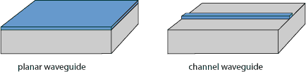
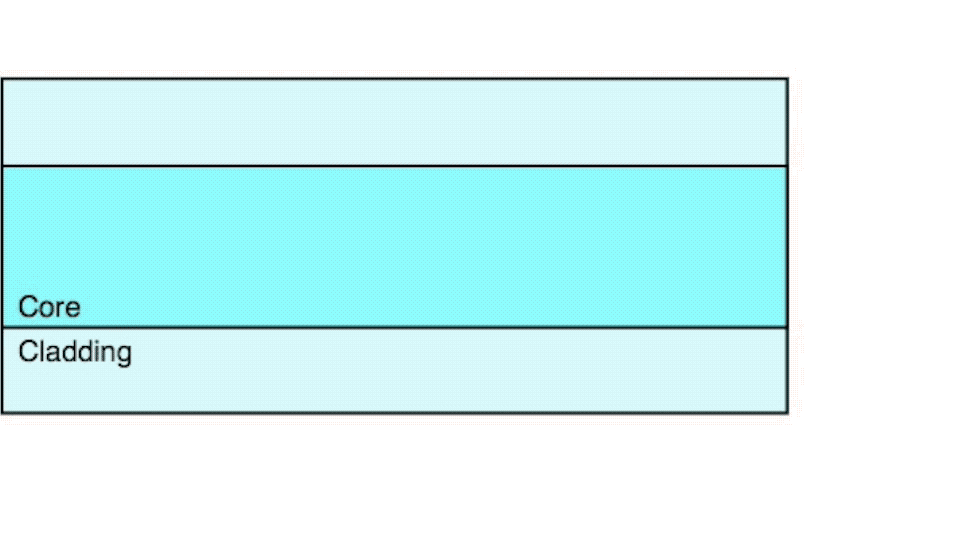
An optical waveguide is a spatially inhomogeneous transparent structure that confines light within a finite region and guides it along a given direction. The most common waveguide has a core region of higher refractive index surrounded by a cladding of lower index, with the light held in the core by total internal reflection. The idea of a waveguide is broader than that of a fibre: a fibre is the commonest cylindrically symmetric waveguide, but there are also planar waveguides (which confine the light in one dimension) and channel waveguides (bar waveguides that confine it in two). In that sense the optical waveguide is the basic physical structure of both integrated photonics and fibre optics.
Table of contents
- 1. What is an optical waveguide? Getting the core concept straight
- 2. Working principle: how an optical waveguide is achieved
- 3. Key parameters: reading the specifications of an optical waveguide
- 4. Main types: what kinds of optical waveguide are there
- 5. Applications: where is an optical waveguide used?
- 6. Common misconceptions: pitfalls to avoid
1. Core concept: what is an optical waveguide?
An optical waveguide is a spatially inhomogeneous transparent structure that confines light within a finite region and guides it along a given direction. The most common waveguide has a core region of higher refractive index surrounded by a cladding of lower index, with the light held in the core by total internal reflection. The idea of a waveguide is broader than that of a fibre: a fibre is the commonest cylindrically symmetric waveguide, but there are also planar waveguides (which confine the light in one dimension) and channel waveguides (bar waveguides that confine it in two). In that sense the optical waveguide is the basic physical structure of both integrated photonics and fibre optics.
2. Working principle: how is an optical waveguide achieved?

The total internal reflection (TIR) is the basis of the light guiding in most optical waveguides. When light travels from an optically denser medium (index n₁) towards the interface with an optically less dense medium (index n₂), and the angle of incidence θ_i is larger than the critical angle θ_c, the light is no longer refracted into the less dense medium but is totally reflected back into the denser one.
💡 The two conditions for total internal reflection
Condition 1: the light must travel from the higher-index medium towards the lower-index one (n₁ > n₂); condition 2: the angle of incidence must exceed the critical angle (θ_i > θ_c). Both are required. Note that the reflection is total, but the optical field does not stay entirely out of the less dense medium — the evanescent wave penetrates the cladding to a certain depth.
Single-mode waveguide
Supports only one transverse mode (the fundamental mode), usually with a small core and a small index difference
Multimode waveguide
Supports several modes or even thousands of them, with a large core or a large index difference
Photonic crystal waveguide
Uses the photonic bandgap effect to confine the light
Surface plasmon waveguide
Uses the surface plasmons of a metal surface and can confine the light on a sub-wavelength scale
Bragg waveguide
Uses the Bragg reflection of a multilayer dielectric film to confine the light
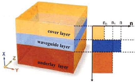
What makes a waveguide work is the confinement of the light. The most common mechanism of confinement is total internal reflection — when light travels from a higher-index medium towards a lower-index one and the angle of incidence exceeds the critical angle, it is reflected completely back into the higher-index medium. By building a “core-cladding” structure (with a core of higher index than the cladding), the light is confined to the core and travels along the axis.
Total internal reflection is, however, only the intuitive picture of geometrical optics; a rigorous description needs wave optics. Inside a waveguide the light exists as discrete modes — each mode corresponds to one transverse electric field distribution that keeps its shape while it propagates (only the phase changes). The modes are obtained by solving Maxwell’s equations together with the boundary conditions of the waveguide.
The number of modes depends on the dimensions of the waveguide and on the index difference:
Besides the total internal reflection waveguides there are other mechanisms of guiding light:
The confinement also brings waveguide dispersion with it — because the light is confined, the wave vector makes an angle with the direction of propagation, and this affects the dispersion. By designing the size and the shape of the waveguide the dispersion can be engineered, which is an important design tool for special fibres such as the photonic crystal fibre.
Waveguide modes: guided, radiation and evanescent modes
The optical field in a waveguide can be divided into different modes, and according to their propagation behaviour there are three families:
① Guided modes: modes that satisfy the condition for total internal reflection and are confined to the core, travelling along the axis of the waveguide. The guided modes are discrete and finite in number, and each has a definite transverse field distribution and propagation constant. A single-mode waveguide supports only one guided mode, a multimode waveguide supports several.
② Radiation modes: modes that do not satisfy the condition for total internal reflection, so the energy radiates away into the cladding and cannot be carried along the waveguide over a long distance. The radiation modes form a continuous spectrum.
③ Evanescent modes: when the waveguide contains a discontinuity (an end face, a bend, a coupler), some fields that decay exponentially in the transverse direction are excited. The evanescent modes do not carry energy along the axis, but they play an important part in near-field interactions such as coupling.
3. Key parameters: reading the specifications of an optical waveguide
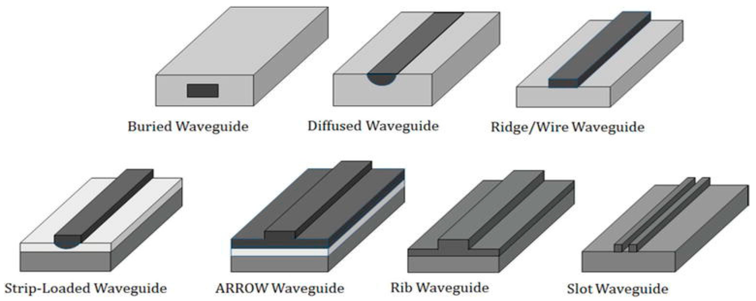
Rib waveguide and ridge waveguide
The two most common structures in integrated optics are the rib waveguide and the ridge waveguide:
① Rib (wire) waveguide: the core is a bar of rectangular cross-section surrounded on all sides by a lower-index material. A rib waveguide confines the light strongly and can be made very small (sub-micron), which suits high-density integration. The scattering loss caused by the roughness of the side walls is, however, more visible as well.
② Ridge waveguide: a raised “ridge” is formed by etching a thicker core layer to confine the light. The mode field of a ridge waveguide is usually larger than that of a rib waveguide, which raises the coupling efficiency to a fibre, and it is also less sensitive to the side-wall roughness and therefore less lossy. It is the waveguide structure commonly used in semiconductor lasers and modulators.
Coupling efficiency and mode field matching
The coupling between a waveguide and a fibre is a key problem in integrated optoelectronics. The coupling efficiency depends on how well the incident field matches the eigenmode of the waveguide, and it can be calculated with an overlap integral:
η = |∫E_fiber · E_waveguide* dA|² / (∫|E_fiber|² dA · ∫|E_waveguide|² dA)
The larger the difference in the size and the shape of the mode fields, the lower the coupling efficiency. The mode field diameter of a single-mode fibre is about 10 μm, while the mode field of a silicon photonic waveguide is usually only 0.3-0.5 μm, so the direct coupling efficiency between the two may be below 10%. In practice a tapered waveguide (spot size converter) or a grating coupler is used to convert the mode field and to couple efficiently.
Core formulas
Mode condition of a symmetric slab waveguide: the light is reflected back and forth between the two interfaces, and the phase matching condition is:
2k₀n₁d·cosθ_m – 2φ_s = 2mπ (m = 0,1,2,…)
where k₀ = 2π/λ is the vacuum wavenumber, n₁ the core index, d the core thickness, θ_m the ray angle of the m-th mode and φ_s the phase shift at total internal reflection.
Normalised frequency: the V number of the waveguide (the normalised thickness) decides how many modes are supported:
V = k₀d√(n₁² – n₂²)
In a symmetric slab waveguide any value of V supports at least one fundamental mode (TE₀ and TM₀); the larger the V, the more modes are supported.
Effective refractive index: the equivalent refractive index n_eff = β/k₀ of a guided mode travelling along the axis, where β is the propagation constant. n_eff lies between n₁ (core) and n₂ (cladding).
Reading the key parameters is the starting point for assessing the performance of an optical waveguide. The table below sets out the main specifications and what they mean:
| Parameter | Meaning | Engineering significance |
|---|---|---|
| Refractive index profile | The refractive indices of the core and the cladding and the shape of the profile | It decides the modal characteristics, the dispersion and the bandwidth of the guide; a graded index profile can markedly reduce the modal dispersion of a multimode guide. |
| Number of modes | The number of guided modes the waveguide supports | Set by the dimensions and the index difference together, it sets how many channels the guide can carry. |
| Effective refractive index | The equivalent refractive index of each mode, linked to the propagation constant | It fixes the propagation constant in the guide and therefore the phase matching conditions and the working wavelength range of the device. |
| Mode field size / effective mode field area | The effective extent of the transverse field distribution | It sets the coupling efficiency to a fibre and the nonlinear thresholds, and is a key parameter in waveguide design and system integration. |
| Transmission loss | The attenuation of the optical power per unit length, in dB/cm or dB/m | The waveguide loss is usually far higher than the loss of a fibre over the same length. |
| Waveguide dispersion | The dispersion introduced by the confinement of the waveguide | It is the dispersion component brought in by the waveguide structure, and the total dispersion can be tuned through the waveguide dimensions and the index profile, which makes it an important tool for dispersion management. |
| Polarisation dependence | The difference in the modal characteristics between the polarisation directions | It shows how differently the guide treats the two polarisation states, which has to be taken into account in coherent communication and in sensing. |
| Bend loss | The additional loss when the waveguide is bent | It sets how tightly the guide may be routed; the smaller the bend loss the better it adapts to compact layouts and the more reliable the system becomes. |
4. Main types: what kinds of optical waveguide are there?
Comparison of the mainstream waveguide material platforms
| Material platform | Index difference Δ | Typical loss | Key advantage | Representative vendors / technology |
|---|---|---|---|---|
| Silica (SiO₂) | 0.3%-2% | <0.1 dB/cm | Very low loss, excellent compatibility with fibres | PLC planar waveguides, AWG |
| Silicon photonics (SOI) | ~40% | ~1 dB/cm | Very high index difference, CMOS compatible, high density integration | Intel, GlobalFoundries |
| Silicon nitride (Si₃N₄) | 20%-40% | ~0.1 dB/cm | Low loss with a moderate index difference, wide transparent window | Ligentec, LioniX |
| Lithium niobate (LN) | ~1% | ~0.1 dB/cm | Excellent electro-optic effect, ultra-high-bandwidth modulators | Thin-film lithium niobate (TFLN) |
| III-V compound semiconductors | ~20% | ~5 dB/cm | Lasers and amplifiers can be integrated monolithically | InP photonic integrated circuits |
| Polymer | 1%-5% | ~0.1 dB/cm | Low cost, flexible, large thermo-optic coefficient | Polymer optical switches |
Optical waveguides can be classified in many ways, and each dimension helps you understand their characteristics from a different angle. The most common ones are introduced below:
By the dimension in which the light is confined
Planar waveguide (confined in one dimension)
The light is confined only in the vertical direction and propagates freely in the horizontal one, as in a thin-film waveguide
Channel / rib waveguide (confined in two dimensions)
The light is confined in both transverse dimensions; this is the basic building block of integrated photonics
Optical fibre (cylindrically symmetric waveguide)
A two-dimensionally confined waveguide of circular cross-section, by far the most widely used waveguide form
By material platform
Silica waveguide
Based on silicon dioxide, low loss, used in communications and with fibres
Silicon waveguide
The core of silicon photonics, with a high index difference, a high degree of integration and operation in the near infrared
III-V semiconductor waveguide
Such as GaAs and InP, able to integrate active devices (lasers, photodetectors)
Polymer waveguide
Flexible to process and cheap, used in specific applications
Lithium niobate waveguide
A strong electro-optic effect and nonlinearity, used in modulators and frequency conversion
Chalcogenide glass waveguide
A high nonlinear coefficient and transparency in the mid-infrared
Sapphire / crystal waveguide
High-power applications
By the mechanism of guiding
Total internal reflection type
The most common type
Photonic bandgap type
Uses a photonic crystal structure
Plasmonic type
Surface waves on a metal, confined on a nanometre scale
5. Applications: where is an optical waveguide used?
The applications of optical waveguides span several fields; the main directions are:
- Optical communication: the optical fibre is itself a cylindrically symmetric waveguide and forms the foundation of the global communication network
- Integrated photonic chips: the waveguide is the “wiring” of photonic integrated circuits in silicon photonics and in indium phosphide, connecting the laser, the modulator, the photodetector and all the other functional devices
- Waveguide lasers and amplifiers: the gain medium is integrated in a waveguide structure to form a compact laser, such as the distributed feedback (DFB) laser
- Optical modulators: lithium niobate and silicon waveguide modulators are the key devices of high-speed optical communication
- Beam splitting and combining devices: power splitters and wavelength multiplexers based on waveguide coupling
- Biochemical sensing: the evanescent field at the surface of the waveguide can be used to detect biomolecules binding at the surface
- Nonlinear optics: the high intensity and the long interaction length in a waveguide make frequency conversion and supercontinuum generation efficient
- Optical phased arrays: beam steering based on an array of waveguides, used in applications such as laser radar
👉 Want to see more real application cases? Visit the application case page of Soar Laser, or contact our technical team directly for professional advice.
6. Common misconceptions
Misconception 1: an optical waveguide is just another name for a fibre
An optical waveguide is the broader concept; the fibre is one particular implementation of it (a cylindrical dielectric waveguide). The term covers any structure that confines light and guides it along a defined direction, including planar waveguides (such as the rib waveguides of silicon photonic integrated circuits), thin-film waveguides, photonic crystal waveguides and surface plasmon waveguides. All fibres are optical waveguides, but not every optical waveguide is a fibre.
Misconception 2: the smaller the waveguide, the better it confines the light
The confinement depends on the index difference and on the size of the structure together, not on the size alone. A small waveguide with a small index difference may confine the light very poorly and may not guide it at all (mode cutoff). Moreover, once the waveguide shrinks to the order of the wavelength or below, a large part of the optical field extends into the cladding (the evanescent field) and the confinement becomes weaker again. Strongly confining waveguides, such as the silicon waveguides with a very large index difference, do reach sub-micron dimensions with strong confinement.
Misconception 3: all waveguides work on total internal reflection
Total internal reflection (TIR) is the most common guiding mechanism, but it is not the only one. A photonic crystal waveguide confines the light with the photonic bandgap effect: a line defect is introduced in a perfect photonic crystal so that light of a given wavelength can only travel along the defect. A surface plasmon waveguide (SPP) is based on the surface electromagnetic wave of a metal-dielectric interface and holds the light on a scale far smaller than the wavelength, while a Bragg fibre guides the light with the multilayer reflector principle. Each mechanism has its own characteristics and its own application range.
Misconception 4: an integrated optical waveguide is just a small fibre
Integrated optical waveguides (such as the silicon photonic and the silicon nitride waveguides) are physically similar to a fibre, but the design philosophy and the process are completely different. A fibre is a cylindrical structure that is drawn, mostly from silica; an integrated waveguide is a planar structure made on a chip by semiconductor processes (lithography, etching, deposition) in silicon, silicon nitride, lithium niobate or a polymer. The advantage of the integrated waveguide is that a large number of waveguides and functional devices (modulators, filters, photodetectors) can be made on the same chip, which gives a photonic integrated circuit.
7. Recommended reading
- What is an optical fibre? How light travels thousands of kilometres in a glass thread
- What is single-mode fibre? Why communication networks use it
- What is active fibre? The fibre that amplifies light
- What is an optical resonator? How do two mirrors trap light?
- What is a solid-state laser? Classic and timeless laser technology
Leave a Reply